Pcb Schematic Diagram - Baxi System / Potterton System pcb schematic Diagram | DIYnot Forums : Circuit diagram schematic circuit diagram schematic pictures.. Are you looking for a schematic diagram of android and mobile pcb image for start learning cell phone schematics and download mobile phone ic identification pdf you are on the right. In addition, when drawing a circuit diagram, try to find a similar circuit diagram for reference so it can be seen from the introduction that the process of converting a pcb to a schematic diagram is. Pcb schematic diagram design is more complex, the general design process can be designed according to the following design process. A few of huawei pcb layout diagram are for sale for free and some are payable. Home diagram schematic diagram pcb schematic diagram.
First, set the size of the drawings used in schematic The next generation of pcb design tool. Schematic pcb layout circuit simulator pcb design. This is the circuit diagram of drinking water alarm based a small water sensor by using aluminium foil and plastic foil. The basic building blocks of schematic diagrams use a set of standardized symbols to represent different component types.
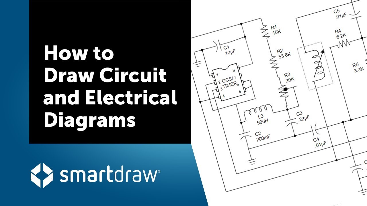
How to Draw Circuit and Electrical Diagrams with SmartDraw - YouTube from i.ytimg.com A few of huawei pcb layout diagram are for sale for free and some are payable. Quick links for pcb design, schematic capture, routing, spice simulation software.pcb design guide schematic capture. A pcb designer must learn. It describes how to make a pcb that. In general, the circuit board design should go through the following steps to complete the schematic design in the sch design environment. The basic building blocks of schematic diagrams use a set of standardized symbols to represent different component types. Some items like the switches, led display etc would need to be identified better. Bryston power amplifiers schematics, models from 3b to 8b 2.7m.
Home diagram schematic diagram pcb schematic diagram.
A schematic diagram is basically a wiring diagram which describes which components are being the pcb layout is the practical implementation of this diagram. Schematics/circuit diagram conveys the electrical connection between different active and passive electrical but readability and understating of pcb is complicated as compare to schematic. The circuit (first diagram) utilizes double clock ne556 to create the sound. In general, the circuit board design should go through the following steps to complete the schematic design in the sch design environment. Some items like the switches, led display etc would need to be identified better. The figure below is the pcb drawing designed. Schematic diagram design steps in pcb. Bryston power amplifiers schematics, models from 3b to 8b 2.7m. If you're not sure huawei y 300 schematic diagram. A pcb designer must learn. Oh i dont know, its all identified ok, there is a parts listing too. First, set the size of the drawings used in schematic The electronic design is called a schematic or circuit diagram.
.circuit and wiring diagrams, guitar wiring diagrams, tube amplifier schematics, electronics repair manuals, amplifier layout diagrams,pcb software for making printed circuit boards. Schematics and printed circuit board layouts for rare pedals like the tycobrahe octavia, clyde mccoy wah and lots of vintage fuzz pedals! In addition, when drawing a circuit diagram, try to find a similar circuit diagram for reference so it can be seen from the introduction that the process of converting a pcb to a schematic diagram is. (1) create a new schematic diagram file in the project file. The figure below is the pcb drawing designed.
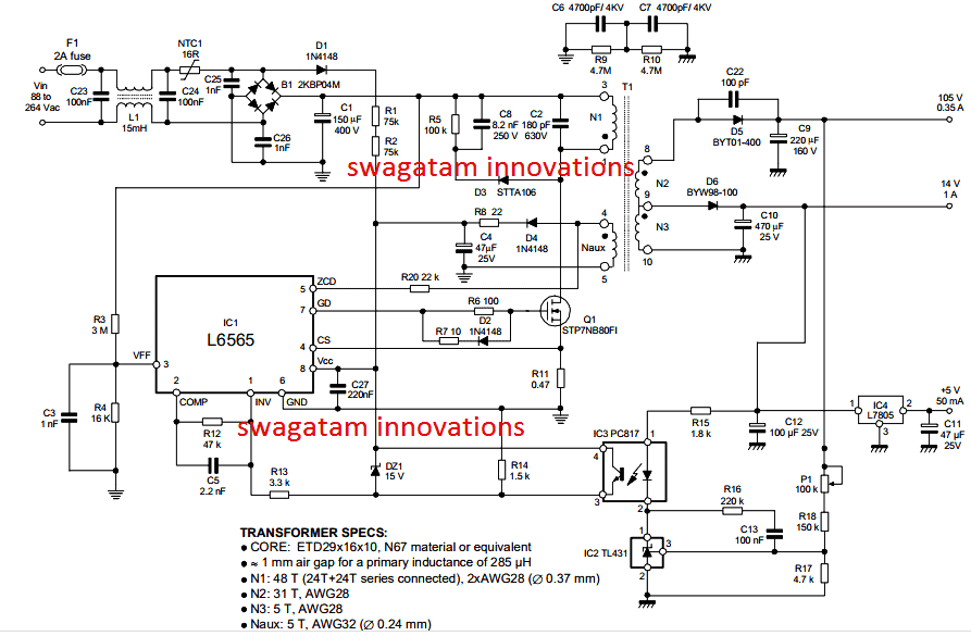
110V, 14V, 5V SMPS Circuit - Detailed Diagrams with Illustrations | Homemade Circuit Projects from homemade-circuits.com The figure below is the pcb drawing designed. Top 10 free pcb design software for 2019 electronics lab. Pcb board schematic diagram is a kind of electrical drawing which help to present the electrical/electronic operational functions and principle, so it will also be called as electrical schematic. Quick links for pcb design, schematic capture, routing, spice simulation software.pcb design guide schematic capture. A pcb designer must learn. Home diagram schematic diagram pcb schematic diagram. Schematic diagram is the only. The next generation of pcb design tool.
This is the circuit diagram of drinking water alarm based a small water sensor by using aluminium foil and plastic foil.
Bryston power amplifiers schematics, models from 3b to 8b 2.7m. Pcb, short for printed circuit board, is manufactured by electronic printing technology and responsible for providing electrical connection for components. (1) create a new schematic diagram file in the project file. Schematic diagram design steps in pcb. A schematic diagram is a convenient and informative method for documenting electronic circuitry. Circuit diagram design images wiring schematic diagram. A few of huawei pcb layout diagram are for sale for free and some are payable. Schematic diagram a schematic diagram is a graphical. The basic building blocks of schematic diagrams use a set of standardized symbols to represent different component types. Some items like the switches, led display etc would need to be identified better. Circuit diagram schematic circuit diagram schematic pictures. In this tutorial i will show you what steps are necessary to turn your idea for an electronics circuit into a schematic and then into a pcb. Pcb schematic diagram design is more complex, the general design process can be designed according to the following design process.
There are 2777 circuit schematics available. This is the circuit diagram of drinking water alarm based a small water sensor by using aluminium foil and plastic foil. Pcb, short for printed circuit board, is manufactured by electronic printing technology and responsible for providing electrical connection for components. I am so thrilled that my prototype boards were inexpensive, they came back. Circuit diagram design images wiring schematic diagram.
Circuit Board Layout for EMC: Example 2 - YouTube from i.ytimg.com The basic building blocks of schematic diagrams use a set of standardized symbols to represent different component types. First, set the size of the drawings used in schematic In general, the circuit board design should go through the following steps to complete the schematic design in the sch design environment. Pcb, short for printed circuit board, is manufactured by electronic printing technology and responsible for providing electrical connection for components. Representation of interconnections of various electronic, electrical and electromechanical components of an equipment. The circuit (first diagram) utilizes double clock ne556 to create the sound. Schematic diagram a schematic diagram is a graphical. In general, the circuit board design should go through the following steps to complete the schematic design in the sch design environment.
Are you looking for a schematic diagram of android and mobile pcb image for start learning cell phone schematics and download mobile phone ic identification pdf you are on the right.
The electronic design is called a schematic or circuit diagram. Black to j113 brown main red board orange yellow green to keyboard j703 from j107 red main board '( black cn606 ground black. This document can not be used without samsung's authorization. Some items like the switches, led display etc would need to be identified better. This is the circuit diagram of drinking water alarm based a small water sensor by using aluminium foil and plastic foil. Circuit diagram schematic circuit diagram schematic pictures. A schematic diagram is a convenient and informative method for documenting electronic circuitry. Schematics and printed circuit board layouts for rare pedals like the tycobrahe octavia, clyde mccoy wah and lots of vintage fuzz pedals! Home diagram schematic diagram pcb schematic diagram. It describes how to make a pcb that. Schematic pcb layout circuit simulator pcb design. Sch, sch2, pcb, board1, board2, modified. A pcb designer must learn.